
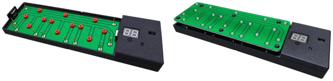
Automated Mainboard Testing Stand Using Stock-Oriented Embedded System Design
Abstract
This paper presents an educational framework for embedded system design based on a stock-oriented component selection strategy. As a practical case study, an automated test equipment (ATE) system was developed on an ATmega328P platform to replace slow manual multimeter testing. By combining I/O multiplexing with smart firmware techniques—such as differential testing for loaded lines and a virtual pull-up for analog inputs—the system overcomes MCU hardware limitations without adding external ICs. The developed prototype reduces testing time to 0.4 seconds per unit—a 22x–42x throughput improvement—while maintaining 100% fault detection accuracy.
Keywords
Embedded Systems, Automated Test Equipment (ATE), Stock-Oriented Component Selection, ATmega328P, Pin Multiplexing, Shared I/O, Non-blocking FSM, Continuity Testing.
Background: Stock-Oriented Methodology
Standard engineering courses usually assume unrestricted component procurement-defining requirements first and purchasing ideal parts later. In contrast, low-budget educational labs and supply-constrained environments require building functional hardware using whatever inventory is on hand. The Stock-Oriented methodology forces the system design to adapt entirely to pre-existing components without ordering dedicated extension ICs.
Industrial Problem Definition
In low-volume manufacturing and educational settings, quality inspection relies on manual digital multimeter (DMM) probing. This approach creates three main operational problems:
Low Throughput: Manual continuity checks take 8 to 20 seconds per Device Under Test (DUT), creating a severe inspection bottleneck.
Operator Error: Human probing is prone to missed test points and inconsistent reading interpretations across multi-pin boards.
Hidden Mechanical Defects: Placing the DUT flat on a workbench during manual probing pushes loose terminal nuts up against PCB vias, masking unfastened hardware and generating false PASS readings.
Commercial ATE platforms solve these issues but are expensive and take time to procure. This project addresses the need for a high-speed, zero-cost ATE stand built under strict microcontroller resource limits.
Core Objectives
Zero Procurement Cost: Deliver a functional ATE platform utilizing strictly existing stock components
Throughput Maximization: Reduce total test cycle time to under 0.5 seconds per unit.
Defect Coverage: Reliably detect electrical opens, shorts, and mechanical hardware assembly faults.
Functional Requirements
Automatic Test Triggering: The system shall automatically initiate a test scan upon mechanical DUT engagement without requiring manual button presses.
Mechanical Fault Exposure: The test fixture shall apply physical contact force to unseat unfastened terminal hardware and reliably expose mechanical assembly defects during probing.
Target Profile Selection: The system shall feature a physical hardware toggle allowing the operator to select between distinct target board profiles.
Multi-Channel Fault Diagnostics: Upon test failure, the system shall report the exact index or channel of any failing node, with support for displaying multiple simultaneous fault locations.
Distinct PASS/FAIL Annunciation: The system shall provide distinct, unambiguous visual and audible feedback to signal test outcome.
Deterministic Loop Timing: The main control loop shall execute with non-blocking logic to maintain system latency under 50 ms.
System Architecture & Hardware Design
Circuit Schematic & Hardware Module Implementation
The system schematic establishes a shared-bus hardware architecture that integrates all measurement probing and user-interface peripherals onto a single ATmega328P microcontroller. Physically, the control hardware is assembled as a "sandwich" stack, combining an Arduino Uno R3 evaluation baseboard with a stacked custom protoboard shield. The schematic is partitioned into five primary functional blocks:
1. Central Microcontroller (Arduino Uno)
The core processor operates at 16 MHz and provides 20 digital/analog I/O lines. Internal registers dynamically switch pin roles between high-impedance input probing during active scanning and active output driving during result presentation.
2. Output Demultiplexer Subsystem (SN74HC138DR)
To expand test channel capacity, an SN74HC138DR 3-to-8 line demultiplexer (U1) is driven by microcontroller pins D11, D12, and D13 (IN0, IN1, IN2). Its active-LOW outputs ( through ) route sequential test pulses to drive channels through across the target board matrix.
3. Single-Pin Analog Control Network (A7)
The analog network encodes both mechanical fixture engagement and target board profile selection into a single analog input (A7):
Resistor Ladder: Resistors (1 k), (2 k), (1 k), and (5 k) form a multi-tap voltage divider
Mechanical Fixture Micro-Switches (SW1, SW2): Wired in series across the network. A valid test scan initiates only when both switches are simultaneously depressed by full, level board insertion.
Configuration Toggle (S3): Selects between Digital and Analog board test profiles by altering the baseline voltage fed into pin A7.
4. Shared User Interface Subsystem
The UI peripherals share physical MCU traces with measurement probes:
7-Segment Displays (S1, S2): Two common-cathode numeric displays driven via bus lines A0–A5, D3, and D4, with common cathodes multiplexed via pins D9 and D10.
Status LED (LD1): Dual-color indicator driven by pins D2 and D6.
Audio Annunciator (B1): Piezoceramic buzzer driven via pin D5.
5. Probing Matrix Interfaces
Drive Probes (–): Mapped directly to outputs – of the SN74HC138DR demultiplexer to supply stimulus signals to the target board.
Sense Probes (–): Connected to MCU pins A0–A6 and D2–D8 to acquire return signals and evaluate trace continuity, voltage drops, and open/short defects
Shared I/O Bus & Multiplexing Architecture
To operate within the 20-pin limitation of the ATmega328P without external port expander ICs, the system uses a shared I/O bus topology. A single set of MCU pins serves a dual purpose:
Active State (DUT Engaged): Pins function as matrix measurement channels using a 74HC138 decoder for line multiplexing.
Diagnostic State (DUT Removed): Releasing the fixture micro-switches reconfigures software register pin directions, converting the same bus to drive user-interface outputs (2-digit 7-segment display, status LEDs, and piezoceramic buzzer).
This physical isolation ensures that measurement lines are never loaded by UI components during active matrix scanning, preventing component loading distorting continuity readings.
Mechanical Probing & Auto-Triggering Fixture
Dual Micro-Switch Sensing: Two series-connected micro-switches detect physical DUT insertion. Both switches must be fully depressed by the board to complete the trigger loop, automatically starting the scan sequence without operator button input.
Mechanical Fault Exposure Geometry: Probing points feature fixed, top-down screwed banana plug fixtures. When the board is pushed into position, top-down mechanical force pushes loose terminal nuts down and away from PCB vias. If a nut is unfastened, this physical force breaks trace contact and triggers an open-circuit failure.
User Interface & Diagnostic Output Hardware
Hardware Profile Switch: A physical 2-state switch connects directly to a dedicated MCU input pin to toggle firmware execution between Digital and Analog board configuration profiles prior to test execution.
Annunciation Peripherals:
PASS Condition: Green LED illuminates, piezoceramic buzzer sounds a 0.1 s pulse, and 7-segment displays 00.
FAIL Condition: Red LED illuminates, piezoceramic buzzer sounds a 0.6 s pulse, and 7-segment displays error indexes.
Diagnostic Fault Display Logic:
Digital Board Profile: Displays static failure codes representing line 1 (d1), line 2 (d2), or both lines (d3).
Analog Board Profile: Displays channel codes (A1 through A8). If multiple channels fail simultaneously, an internal software buffer cycles through all active error codes sequentially on the 7-segment display at a 1 Hz refresh rate.
Firmware Architecture & Software Design
Finite State Machine Architecture & State Machine
The system firmware operates as a deterministic, event-driven Finite State Machine (FSM). To maintain absolute system responsiveness without blocking execution loops, all peripheral tasks—such as display multiplexing, switch debouncing, audio annunciation, and analog sampling—are scheduled using timestamp comparison routines (millis()). The FSM decouples physical measurement from user-interface rendering, ensuring that the shared physical bus is dynamically reconfigured in direct synchronization with the active operational state.
Detailed State Execution & Transition Dynamics
APP_IDLE State
Execution Logic: The MCU continuously runs background schedulers (3 ms display refresh, 10 ms audio handler, 50 ms configuration poll). Display rendering is active (displayEnabled = true). If a previous run resulted in TEST_FAIL with multiple identified fault channels, a 1000 ms non-blocking timer iterates through stored failure codes to cycle diagnostic indices across the display.
Transition Condition: The system samples the single-pin analog network (CONFIGURATION / A7). When downward fixture pressure depresses both series micro-switches, the voltage drops below the active threshold, setting appState = APP_START_TEST.
APP_START_TEST State
Execution Logic: The firmware immediately isolates the shared bus by disabling display multiplexing (displayEnabled = false) and driving display cathode lines high. It resets the evaluation status to TEST_NONE, clears fault registers (failedCount = 0), and latches the active target profile (activeBoardIsDigital). Initial pin directions for testing are applied.
Transition Condition: Upon completing bus isolation and register initialization, the FSM immediately advances to appState = APP_TEST_RUNNING within the same execution loop.
APP_TEST_RUNNING State
Execution Logic: The MCU periodically executes matrix evaluation tasks at 50 ms intervals (DigitalTask() or AnalogTask()). It steps through the 74HC138 demultiplexer channels, evaluating trace continuity. Based on the matrix evaluation, the firmware sets testResult to either TEST_PASS or TEST_FAIL and populates the failure buffer with specific line indices (d1–d3 for Digital, A1–A8 for Analog).
Transition Condition: Matrix scanning continues continuously until the operator extracts the board. Releasing the fixture opens the micro-switches, returning the A7 voltage to its unengaged level and transitioning the FSM to appState = APP_SHOW_RESULT.
APP_SHOW_RESULT State
Execution Logic: The MCU re-enables UI display rendering (displayEnabled = true) and restores shared pins (PD2, PD6, PD5) to output driver mode. It evaluates testResult:
TEST_PASS: Green LED illuminates, a 100 ms audio pulse is triggered, and the display buffer loads 00.
TEST_FAIL: Red LED illuminates, a 600 ms audio alarm pulse is triggered, and the primary failure code is loaded into the active display buffer.
Transition Condition: After triggering peripheral indicators, the FSM automatically resets appState = APP_IDLE, returning to idle monitoring or multi-fault display cycling.
Advanced Signal Measurement Routines
Differential Line Sampling (ReadDifferential):
Standard logic reads fail on traces containing inline active components (such as indicator LEDs or buzzers) due to non-linear forward voltage drops. The firmware executes a two-phase differential check by toggling the 74HC138 demultiplexer between its active channel and an inactive channel with a 10 s settling delay:
This pulse verification isolates true conductor continuity from semiconductor forward voltage drops without false-positive open circuit readings.
ADC Sample-and-Hold Capacitor Flushing (ReadAnalogA6):
Channel A6 lacks internal digital pull-up resistors (INPUT_PULLUP). The firmware executes a dummy analogRead conversion prior to sampling. This clears and pre-charges the internal ADC sample-and-hold capacitor (~14 pF), establishing a stable software virtual pull-up without requiring discrete external resistors on the circuit board.
Multi-Fault Diagnostic Cycling Engine
When an Analog profile check detects multiple failing channels, all failing channel indices are stored in a failure array during APP_TEST_RUNNING. Upon transitioning to APP_SHOW_RESULT and returning to APP_IDLE, a 1000 ms timer continuously iterates through all recorded error codes, rendering diagnostic indices (A1 through A8) sequentially on the two-digit display at a 1 Hz refresh rate.
CAD Enclosure & Mechanical Design
Parametric SolidWorks CAD Modeling & Manufacturing Strategy
The benchtop chassis was designed in SolidWorks and fabricated using additive FDM manufacturing on a Bambu Lab 3D printer. Because the total axial length of the ATE chassis exceeded the physical build plate volume, the enclosure model was strategically partitioned into two interlocking split-body sections that join along a precision mechanical seam. Integrated alignment tabs along the joint ensure structural rigidity, precise axial registration, and seamless post-print assembly.
Dual-Domain Structural Architecture
The chassis layout is physically divided into two distinct functional domains to isolate the test fixture from the sensitive control electronics:
Control & UI Domain (Right Part):
An elevated box module designed to enclose the controller assembly and present the user interface.
DUT Probing Domain (Left Part):
An elongated, open-top bay designed to securely position the target circuit board under test. This section houses the fixed probe bed and recessed micro-switches, absorbing top-down mechanical probing pressure during board insertion without transferring mechanical stress to the control electronics.
Experimental Results & Performance Verification
The fully assembled ATE platform was evaluated across physical, electrical, and real-time execution parameters.
Operational Speed & Throughput
The automated ATE platform was evaluated against standard manual digital multimeter (DMM) continuity probing across target circuit boards (Digital and Analog variants). Manual inspection required an operator to manually position handheld probes across test points, consult wiring schematics, and record line continuity point-by-point. The automated platform executes the full matrix scan automatically upon physical fixture engagement.
Scan Time: Manual probing required approximately 8 s to 20 s per board. The ATE platform completes a full matrix scan in under 0.4 s once the micro-switches engage.
Diagnostic Output: Fault identification occurs immediately upon board extraction, displaying designated error codes (d1–d3 for Digital, A1–A8 for Analog) without requiring manual trace tracing.
Cost Efficiency: The platform achieved full functionality at zero capital expenditure ($0.00), constructed entirely from existing laboratory stock parts (ATmega328P, 74HC138 demultiplexer, 7-segment display, and 3D-printed enclosure).
Functional Verification & Defect Coverage
System verification was conducted using target test boards across four primary operational conditions:
Electrical Open & Short Circuits: Direct logic scanning across the 74HC138 matrix channels successfully identified open traces and bridge shorts across test channels.
Mechanical Fastener Verification: Target boards with unfastened terminal nuts were tested on both a flat bench setup and the ATE fixture. On a flat bench, upward normal force from the work surface kept loose nuts flush against PCB vias, producing false PASS readings during manual DMM checks. On the 3D-printed ATE stand, top-down pressure from the fixed banana plug probes physically pushed unfastened nuts downward away from the vias, breaking trace continuity and triggering a true FAIL result.
Firmware Real-Time Task Timing
Microcontroller task timing was verified against non-blocking loop constraints. The Finite State Machine (appState) executed background tasks—including 3 ms display multiplexing, 10 ms audio/button handling, and 50 ms analog A7 network sampling—without hardware-halting delays, maintaining main loop execution well below the 50 ms timing threshold.
Conclusion & Future Scope
Conclusion
The project successfully realized an automated test equipment (ATE) platform using an ATmega328P microcontroller and existing stock laboratory components. By leveraging shared I/O pin busing, 74HC138 demultiplexing, and single-pin analog voltage encoding, the system maximizes hardware utility within strict MCU pin constraints. Specialized firmware routines—including differential pulse sampling and ADC sample-and-hold capacitor pre-charging—reliably evaluate loaded lines and un-tempered analog channels without requiring extra BOM components. The Bambu Lab 3D-printed SolidWorks enclosure physically isolates the control sandwich PCB from probing stress, while top-down mechanical fixture pressure reliably exposes loose terminal hardware that manual DMM probing misses.
Future Scope
Non-Volatile Logging: Adding EEPROM or SD card storage to log diagnostic failure history and unit serial numbers for quality control tracking.
Automated Clamping: Replacing manual board insertion pressure with a pneumatic or motorized mechanical latch.