
0. Abstract
Printed Circuit Board Assemblies (PCBAs) are critical components in modern electronic devices, where reliability and longevity are so important. We all know that the primary main points related to quality and reliability in electronic applications and products lies in to five main areas:
Good Embedded Design (Schematic, PCB, Firmware Software)
Good Mechanical Design (Solid and Thermodynamic)
Simulation and Analyze
Good DFM (Design for Manufacturing) Design
Using good quality Components in production
However, also some other secondary critical and sometime hidden factors remain which contribute to long-term failures that can compromise the performance. This paper explores secondary causes factors behind these failures, including ESD, Thermal stress, Mechanical stress, Flux contamination, poor soldering practices, and environmental influences such as moisture and so on. Each factor described for its impact on PCBA reliability, emphasizing how material degradation, improper handling, and poor control manufacturing and assembling processes effected on long-term issues. Effective strategies, such as accurate soldering techniques, general handling during production and robust testing protocols, are discussed to enhance durability and reduce failure rates. By understanding these failure mechanisms, manufacturers (in any scale from prototyping to mass production) can implement best practices to ensure the reliability and flexibility of PCBAs in different applications.
1. ESD Damages in PCBA and Electronic Components
Electrostatic discharge (ESD) can severely affect PCBA reliability during production and handling if proper precautions are not taken. The following details focus on decreasing ESD risks specific to production processes and PCBA handling. Even if conditions and materials all are in standard scope, static discharge can occur and can it quickly rise to kilovolts. Components often cannot handle this kind of discharge and so it is vital not to let the discharge build up too much. Damage caused by ESD cannot always be determined immediately (Called Direct Faults). It is highly probable that the component will function fine at first and then fail inexplicably weeks or month later (Called Latent Faults).
It is so important to take in account that less than 30% of all damaged caused by ESD event is direct damaged and latent damages have much higher share about 70%.
Below you can see a picture of a damaged chip using electron microscope, showing how small-scale the damage often is.
Because the damage often only becomes noticeable later on, it regularly happens that products suddenly fail after being in use for some time.
When a device is in use, all electrical connections are protected against ESD. However, working on PCBs without housing, exposes the circuit boards to ESD at places that are not protected.
1.1 Main Causes on ESD Damage
1.1.1. Improper Handling by Personnel
ESD-sensitive PCBAs are often damaged when handled by untrained personnel without proper grounding. Static electricity from the human body can discharge into the board, leading to latent or immediate failures.
1.1.2. Inadequate ESD-Safe Workstations
Workstations without ESD-safe surfaces or grounding mechanisms allow static charges to accumulate and transfer to PCBAs. This includes workbenches, chairs, and tools that do not comply with ESD standards.
1.1.3. Unprotected Equipment
Machines and tools used in production, such as conveyors, pick-and-place machines, reflow ovens and hand Soldering units can generate static electricity if not properly grounded or maintained, creating a high-risk environment for ESD events.
1.1.4. Environmental Conditions
Dry environments with low humidity levels increase the likelihood of static charge buildup on personnel, equipment, and materials. Without control measures like ionizers or humidifiers, static discharge risks are amplified.
1.1.5. Improper Storage and Transport
PCBAs stored or transported in non-ESD-safe containers, such as regular plastic bags or ungrounded trays, are vulnerable to static buildup and discharges during movement or handling.
1.1.6. Assembly Processes
Manual assembly operations, such as soldering or inspection, can introduce ESD damage if performed without protective measures. Even the use of certain cleaning agents can generate static electricity, posing risks to PCBAs.
1.2 Conclusion
Assembly processes, particularly those involving manual intervention, are a major source of ESD risks. Implementing robust control measures, training personnel, and maintaining ESD-safe environments can significantly reduce failures and improve the long-term reliability of PCBAs.
Interesting Link on this topic on YouTube:
https://youtu.be/bWXNOemu2j4?si=0-EpfCX6qIfsu2P
2. Flux Contamination in PCBA and Components
Flux contamination during PCB production is not only influenced by flux handling but also by the soldering process itself. Remaining flux from improperly managed soldering processes can significantly impact the PCB’s long-term reliability. When engineers speak of flux residue, they are referring to the risk of failure, not the chemistry of the flux or residue itself. No single term or single test captures all the information required to understand this type of risks. What is understood is that as circuits continue to work on longer periods of time, the risk of failure increases.
2.1 Impact of flux contamination
Surface insulation resistance - Affects electrical measurement accuracy and generate parasitic electrical paths
Contamination of sensitive parts (Connector, Switches, Sensors, …) - Couse to early break down of mechanical categorized components
Inadvertent creation of a conductive path between nearby traces - Accelerate electrical breakdown of traces. Resulting in potential damage the circuit
2.2 Parasitic electrical paths
An ideal printed circuit board has no impact on a circuit’s performance but in reality, certain PCB layout, electronic components, and other materials create extra circuit elements, known as Parasitics!
Migration From Design (Simulation) to Reality
2.2.1. Effects on measurements
Excess solder flux on PCBs and components can cause DC voltage errors and unpredictable behaviors in frequency domain. See image below.
2.3. Main Causes on Flux Contamination
2.3.1. Incomplete Cleaning
Flux residues not carefully removed after soldering remain on the PCB surface. During soldering, the high temperatures can affect the composition of the flux, making it harder to clean. If the cleaning process doesn’t match with the flux, cleaning becomes less effective, leaving harmful residues on the board.
2.3.2. Improper Flux Selection
Selecting a flux incompatible with the application and soldering process or board materials can lead to excess residue that is challenging to clean. For example, Low-activity flux may not work well in high-temperature soldering or High-residue fluxes used in wave or selective soldering without sufficient cleaning can lead to corrosion.
2.3.3. Overuse of Flux
Excessive flux application during the soldering process often occurs in wave soldering or manual soldering due to overloaded flux spray systems or manual application errors. This overuse results in more residue being left behind, especially if the heating process isn’t optimized to burn off excess flux during reflow.
2.3.4. Residue Trapped Under Components
The soldering process can cause flux residues to flow under tightly packed components or low-profile devices, where they solidify and become unreachable by traditional cleaning methods. In reflow soldering, uneven heating can worser this issue, as flux residues may migrate to inaccessible areas under thermal stress. These residues can later reactivate in humid environments, leading as corrosion or electrical leakage.
2.3.5. Environmental Factors
The soldering environment itself, including temperature and humidity, plays a significant role in flux residue formation. Poor control of soldering temperatures can cause flux to leaving behind hard-to-clean residues. Additionally, an unregulated environment during soldering or cooling can promote moisture absorption into flux residues, increasing the risk of corrosion or leakage.
2.3.6. Lack of Process Control and Monitoring
Insufficient control over reflow oven profiling and soldering parameters (such as time, temperature, and flux activation) can lead to incomplete flux activation or carbonization.
2.4. Conclusion
Flux contamination during production is closely linked to the soldering process. Managing soldering parameters effectively, selecting the right flux for the process, and implementing rigorous cleaning and inspection protocols can significantly reduce the risks of contamination. Ensuring compatibility between soldering methods and flux properties, combined with robust environmental and process controls, is key to long-term PCBA reliability.
Interesting Link on this topic on YouTube:
https://www.youtube.com/watch?v=nyUt9p0xbtE
3. Popcorn Effect/Defect in Electronic Components
In short, the popcorn effect is when the IC or BGA blows up or even breaks because the moisture inside the bundle grows in the reflow interaction. The popcorn effect/defect is a critical failure mechanism in moisture sensitive electronic components that not only causes immediate physical and electrical damage but also leads to long-term reliability issues. It occurs during high-temperature soldering or reflow processes, where trapped moisture inside the component expands into steam, leading to internal damage. This defect can result in latent failures that manifest over time due to structural and electrical degradation within the component.
3.1. Main Causes on Popcorn Effect
3.1.1. Moisture Absorption
Moisture sensitive devices (MSDs) absorb moisture from the environment over time, especially when stored in high humidity conditions without proper protection. Also, the packaging materials of components, such as plastic encapsulants, are hygroscopic and can retain water.
3.1.2. Rapid Heating During Soldering
During the reflow soldering process, the component is exposed to high temperatures (e.g., 200°C–280°C) which cause moisture inside the package turns into steam and expands rapidly and creating internal pressure. The internal pressure caused by the expanding moisture exceeds the mechanical strength of the encapsulated material which can cause to cracks, delamination, or physical deformation.
3.2. Effects of Popcorn Defect
3.2.1. Delamination: Layers within the component can separate, leading to weakened structural integrity.
3.2.2. Cracks in the Package: Cracks expose the die and internal components to environmental factors like moisture and contaminants, leading to long-term failures.
3.2.3. Electrical Failure: Internal damage can lead to open circuits, short circuits, or degraded electrical performance.
3.2.4. Mechanical Damage: The component may become completely unusable due to physical deformation or detachment from the PCB.
3.3. Prevention of Popcorn Defects
3.3.1. Proper Storage of Moisture Sensitive Devices (MSDs)
Store components in dry cabinets (under controlled storage conditions with relative humidity below 10%) beside humidity indicator cards. Also use vacuum-sealed packaging to minimize moisture exposure.
3.3.2. Bake Procedures
Before soldering, bake moisture-sensitive components in a controlled oven to remove absorbed moisture if they need by follow the IPC standards (IPC-JEDEC J-STD-033B) for bake recommendations on time and temperature.
3.3.3. Use of Moisture Sensitive Labels (MSLs)
Follow the Moisture Sensitivity Level (MSL) guidelines provided by manufacturers. MSL classifications ranges from 1 (not moisture sensitive) to 6 (extremely moisture sensitive) which should be handled according to their specified MSL and instructions come from IPC standards.
3.3.4. Controlled Soldering Processes
Use reflow profiles optimized for gradual heating to reduce the risk of rapid moisture expansion by avoiding excessive peak temperatures (4 at image below) during reflow soldering and extending preheat phase (1 at image below).
3.3.5. Inventory Management
Track the floor life of components once removed from dry packaging and use only components within their allowable exposure time (as specified by the MSL and IPC standard).
3.4. Conclusion
The popcorn defect poses a significant threat to the reliability of moisture-sensitive electronic components, causing immediate damage during soldering and long-term failures due to internal cracking and delamination. These latent defects can lead to reduced insulation resistance, increased susceptibility to environmental stress, and eventual component breakdown in the field. Proper storage, handling, and process control such as baking, adhering to MSL guidelines, and optimizing soldering profile are critical to preventing both immediate and long-term issues. By addressing these risks, manufacturers can ensure the durability and reliability of their PCB assemblies over time.
4. Thermal Stress on PCBA and Components
Thermal stress is a significant issue to long-term PCBA failures. It arises from the expansion and contraction of materials when exposed to temperature fluctuations during operation or manufacturing processes. Over time, this cyclical stress can degrade the mechanical and electrical integrity of a PCB, leading to critical failures.
Effect of Environmental Exposure Stresses
4.1. Main Causes on Thermal Stress
4.1.1. Thermal Cycling and High-Temperature Operation
Repeated heating and cooling cycles during product normal operation or be in environmental exposure stresses from one side and continuous exposure to elevated temperatures in high-power or heat-generating devices on the other side are two common problems on this issue.
4.1.2. Hotspots on the PCB and Thermal Mismatch
Uneven heat distribution due to localized high-power components caused localized stress. This issue become much more worser when different materials such as copper, solder, aluminum and laminate (which have different coefficients of thermal expansion CTE) used in a PCBAs. This mismatch causes stresses during temperature changes, especially at critical points like solder joints and component pads.
4.1.3. Manufacturing Processes:
Rapid temperature changes during soldering (Manual soldering, Reflow or Wave soldering) which normally comes incorrect setup of temperature profile on different stages like preheating, Soldering and cooling.
4.2. Effects of Thermal Stress
4.2.1. Solder Joint Cracking
Repeated expansion and contraction weaken solder joints over time, leading to microcracks or detachment. BGAs and SMDs joints are particularly effected. This microcracks or stress in conductive paths increase resistance, causing signal integrity issues or power loss.
Image below shows a comparison of cross-sections before and after a thermal shock test with 3000 cycles. It is clear that the solder of the regular terminal product has deteriorated more than of Stack type called MegaCap.
4.2.2. Delamination
Layers within the PCB can separate due to excessive thermal stress. This delamination disrupts electrical connectivity and increases the risk of corrosion.
4.2.3. Material Fatigue
The materials used in components, Solder joints and PCB laminate can lose its mechanical strength, leading to warping or microcracks in traces and vias which cause acceleration in material aging. Image below shoes this effect on solder joints of BGA component.
4.2.4. Component Damage
Heat-sensitive components can degrade or fail when facing with cyclical high temperatures over time. Components like capacitors and ICs lose their normal functionality due to these types of stress.
4.3. How to Detect Thermal Stress Damage
Detecting thermal stress damage in PCBAs requires a combination of visual, mechanical, and electrical testing methods to identify underlying issues. X-ray inspection is widely used to detect microcracks in solder joints, voids, and delamination within the board's layers. Thermal imaging can pinpoint hotspots (image below at left) and uneven heat distribution (image below at right) that might indicate stress-prone areas. Acoustic microscopy is a non-destructive method to identify delamination or voids within the PCB.
4.4. Prevention of Thermal Stress
4.4.1. Material Selection
Use materials with compatible coefficients of thermal expansion (CTE) to minimize thermal mismatch. For example, for PCbs select high-Tg (glass transition temperature) laminates to operating in high-temperature environments and for components chose high grade temperature classes which can be operatable in high-temperature environments.
4.4.2. Effective Thermal Management
- Heat Dissipation: Incorporate heat sinks, thermal vias, or heat spreaders in the PCB design.
- Thermal Interface Materials: Use high-quality thermal pastes or pads to improve heat transfer from components. - Cooling Solutions: Implement active/forced or passive/natural convection cooling methods to control temperature (see images below).
The behavior of overall system can also be simulated by heat transfer analyses (HTF) tools in design phase to minimize the cost in prototyping.
4.4.3. Optimized PCB Design
Distribute high-power components evenly to avoid hotspots and use wider traces or additional copper layers to improve heat dissipation.
4.4.4. Manufacturing Process Control
Optimize soldering temperature profiles to minimize thermal shock ensuring gradual heating to reduce thermal stress during soldering. Selecting the best match solder paste to application is also one of the main factors to overcome these types of problems.
4.4.5. Conformal Coating
Apply a conformal coating to protect the PCB from environmental stress, such as moisture, chemical exposure, and temperature variations. Conformal coatings help to stabilize the PCB structure by reducing the impact of rapid thermal changes and providing additional insulation to critical areas. Selecting heat-resistant coating materials, such as silicone-based or parylene, for high-temperature applications can be so helpful to overcome these types of problems.
4.4.6. Regular Maintenance
Inspect high-power assemblies periodically for signs of thermal damage or stress and replace components or boards showing significant wear or fatigue.
4.5. Conclusion
Thermal stress is a critical factor that impacts the long-term reliability of PCBAs. It can lead to solder joint cracking, delamination, material fatigue, and component failures. By employing effective thermal management techniques, selecting suitable materials, and optimizing manufacturing processes, manufacturers can significantly mitigate thermal stress and enhance the durability of their PCBAs.
5. Mechanical Stress on PCBA and Components
Mechanical stress is a significant cause of long-term PCBA failures, arising from forces applied during manufacturing, handling, or operation. These stresses can lead to physical damage to the PCB, its components, and solder joints, compromising the assembly's structural and electrical integrity over time.
Effect of Environmental Exposure Stresses
5.1. Main Causes on Mechanical Stress:
5.1.1. Vibration
Common in applications like automotive, aerospace, or industrial machinery where PCBAs are exposed to continuous or intermittent vibrations. Vibrations can loosen solder joints, damage traces, or crack components.
5.1.2. Shock and Impact
Sudden mechanical impacts during transportation, handling, or operation can damage solder joints, components, or the PCB substrate.
5.1.3. PCB Flexing
Bending or warping of the PCB due to improper handling during assembly or installation. This issue has more impact on larger PCBs or those with heavy components.
5.1.4. Improper Mounting
Using incorrect mounting hardware or techniques can induce localized stress on the PCB, leading to cracks or warping. Excessive tension also can be applied on connectors or cables during attachment to the PCBAs.
5.2. Effects of Mechanical Stress
5.2.1. Cracked Solder Joints: Vibrations or flexing can weaken solder joints, causing microcracks or complete detachment of components.
5.2.2. Trace Damage: Mechanical stress can cause breaks in copper traces, leading to open circuits or intermittent connections.
5.2.3. Component Failure: Physical stress on surface-mount or through-hole components can cause fractures or misalignment which will impacting functionality.
5.2.4. Connector or Pad Detachment: High-stress areas like connectors can peel away from the PCB, causing operational failures.
5.3. How to Detect Mechanical Stress Damage
Detecting mechanical stress damage in PCBAs requires a combination of visual, mechanical, testing methods to identify underlying issues. X-ray inspection is widely used to detect microcracks in solder joints and components.
5.4. Preventing Mechanical Stress
5.4.1. PCB Design Optimization
Use thicker PCBs or higher-quality laminates for improved rigidity. Adding support structures like mounting holes or stiffeners for large or heavy PCBs can overcome these types of problems too. Also avoid placing critical components near PCB edges or mounting points. During PCBs depanelizing the unpredictable stress can apply to components which are installed near the PCB edges or breaking axis.
5.4.2. Component Mechanical fixing
Fixing components like large capacitors, connectors, or inductors with adhesive or additional solder on PCB.
In harsh environments applications where natural vibration and mechanical stresses always exists its recommended to use underfill material for BGA and other sensitive components to distribute mechanical stresses.
5.4.3. Proper Handling and Assembly
Train manufacturing personnel to handle PCBAs carefully to avoid bending or flexing using appropriate tools and fixtures during assembly to prevent unnecessary mechanical stresses.
5.4.4. Connector and Cabling Management
Ensure cables and connectors are strain-relieved to prevent stress on solder joints and pads. Using locking connectors or secure cable ties to avoid accidental pulling or tension can extremely overcome on connection related problems.
5.4.5. Testing and Validation
Perform vibration and drop tests to simulate real-world mechanical stresses. Also, some simulation tools like finite
element analysis (FEA) during the design phase can help to identify and mitigate high-stress areas in PCBAs.
5.5. Conclusion
Mechanical stress is a critical factor in long-term PCBA failures, causing damage to solder joints, traces, and components. Proper design, careful handling, and robust testing methods can significantly reduce the risks associated with mechanical stress. By addressing these factors early in the design and manufacturing process, manufacturers can ensure the durability and reliability of their products in demanding environments.
6. Effects of Poor Soldering in PCBA and Components
Bad soldering practices, including cold soldering, insufficient solder, excessive solder, or improper reflow profiles, can have a significant impact on the long-term reliability of PCBAs. Soldering defects weaken the structural and electrical integrity of the assembly, making it more prone to failures over time, especially in harsh and demanding environments.
6.1 Main Causes on Poor Soldering:
6.1.1 Cold Solder Joints
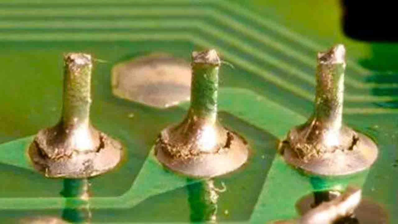
This issue caused by insufficient heat during the soldering process, resulting in incomplete or weak bonds. Having cold
solder joints leads to high resistance, intermittent connections, and mechanical failures over time.
6.1.2 Insufficient Solder
Insufficient solder application leads to poor mechanical support and incomplete electrical connections. These types of defected joints are prone to detachment under mechanical stress or thermal cycling.
6.1.3. Excessive Solder
Excessive of solder can cause bridging between adjacent pads or components, leading to short circuits. This defect can also increase the likelihood of solder balls or spatter, which can cause intermittent electrical faults.
6.1.4. Voids and Inclusions
Voids in solder joints occur due to trapped air or flux residues during reflow. These voids weaken the joint and reduce its ability to conduct heat or electricity.
6.2. Effects of Bad Soldering
6.2.1. Intermittent Connections: Weak or incomplete solder joints can cause sporadic electrical connectivity issues, leading to erratic device behavior.
6.2.2. Mechanical and Thermal Failures: Poorly soldered joints lack the structural strength to endure mechanical and components may detach or connections may fracture over time. Also, poor solder joints are more susceptible to cracking or delamination under thermal cycling. This is particularly problematic in high-power or high-temperature applications.
6.2.3. Increased Resistance: Incomplete or poorly formed joints have higher electrical resistance, leading to power loss, signal degradation, and overheating.
6.2.4. Short Circuits and Open Circuits: Excess solder can create unintended connections between adjacent pads, while insufficient solder can lead to open circuits over time.
6.3. How to Detect Poor Soldering Joints
Detecting Poor Soldering Joints in PCBAs requires a combination of visual, testing methods to identify underlying issues. X-ray inspection is widely used to detect microcracks in solder joints and components.
6.4. Preventing Poor Soldering in PCBAs
6.4.1. Optimized Soldering Processes
Ensure soldering irons, wave soldering machines, and reflow ovens are properly calibrated for the chosen solder alloy or paste. Use accurate and consistent temperature profiles for reflow soldering which compatible with PCBA, Application, Standards and Solder paste itself. Apply solder precisely using automated dispensing or stencil printing to avoid over- or under-application and inspect solder paste deposition for consistency before soldering.
6.4.2. Surface Preparation
Clean PCB pads and component leads to remove oxidation, dirt, or grease before soldering. Use complimentary flux to improve solder wetting and bonding based on solder paste, PCB and components stocking situation.
6.4.3. Operator Training
Train operators on proper soldering techniques and the importance of maintaining consistent heat and solder application.
6.4.4. Inspection and Testing
Implement automated optical inspection SPI, AOI and X-ray inspection for early detection of soldering defects.
6.5. Conclusion
Poor soldering practices are a major contributor to long-term PCBA failures, causing intermittent faults, mechanical detachment, thermal fatigue, and electrical inefficiencies. By implementing robust soldering processes, thorough
inspections, and operator training, manufacturers can minimize the risks associated with poor soldering and ensure the long-term reliability of their PCBAs.
7. Effects of Buggy Firmware Software
Firmware and software play a critical role in the functionality and reliability of modern PCBAs. Buggy or poorly written firmware can significantly impact the long-term reliability of electronic devices, causing operational failures, hardware stress, and premature degradation of components.
1.1 Main Causes on Buggy Firmware Software
Buggy firmware or software is often caused by insufficient testing during development, which allows undetected bugs to persist into production. Poor error handling mechanisms can result in unresponsive systems or cascading failures, while inefficient resource management, such as improper allocation of memory or power, can overburden hardware components. Compatibility issues arise when firmware is not tailored to the specific hardware configuration, leading to operational mismatches. Additionally, untested updates and patches can introduce new bugs, and poor coding practices, such as a lack of modularity or maintainability, increase the likelihood of errors in complex systems. Collectively, these factors contribute to software instability and long-term reliability issues for PCBAs.
1.2 Effects of Buggy Firmware/Software
7.2.1. Excessive Wear on Components
Incorrectly programmed firmware can cause components like microcontrollers, memory chips, or power regulators to operate outside their designed specifications, leading to overheating, overloading, or accelerated aging.
7.2.2. Increased Power Consumption
Inefficient power management in firmware can cause batteries to drain quickly or induce thermal stress in power components, reducing their lifespan.
7.2.3. Memory Corruption
Bugs in memory handling can lead to data corruption, affecting system functionality and potentially causing permanent damage to memory cells.
7.2.4. Recurrent System Crashes
Continuous system reboots or crashes due to firmware issues increase mechanical stress on components and system overall reliability.
7.2.5. Communication Failures
Buggy firmware can disrupt communication protocols, causing peripherals or external devices to function incorrectly, leading to intermittent failures or complete loss of functionality.
7.2.6. Security Vulnerabilities
Firmware bugs can expose the system to hacking or being Ciber attacks, which may lead to operational failures or permanent hardware damage.
7.2.7. Unintended Behavior
Bugs may cause components to perform tasks they were not designed for, leading to unexpected stress or failure modes in the hardware.
1.3 How to Detect Firmware/Software Issues
Detecting firmware or software issues requires comprehensive testing and monitoring techniques. System-level testing on real hardware under simulated operating conditions helps detect bugs that may not appear in virtual environments. Debugging tools and logging systems are essential for tracing execution paths and capturing unexpected behaviors. Stress testing pushes the system to its limits to identify issues under extreme conditions, while
functional testing ensures the firmware meets its intended specifications. Field monitoring and collecting logs from deployed systems provide valuable insights into long-term issues, enabling developers to identify and address problems that arise during real-world usage.
1.4 Preventing Buggy Firmware/Software
Preventing buggy firmware or software requires a combination of continues testing, robust development practices, and also continuous monitoring. Comprehensive testing procedures, including unit, integration, and system-level testing, ensure that the firmware performs as expected under real-world conditions. Implementing error handling mechanisms allows the system to recover from unexpected issues, while optimizing resource management ensures efficient use of power, memory, and processing cycles. Adhering to coding standards, such as modular design and getting reviews, enhances code quality and maintainability. Additionally, validating firmware compatibility with specific hardware configurations and using diagnostic tools for continuous monitoring help to identify and resolve potential issues early, ensuring reliable and durable operation over the product's lifecycle.
7.5 Conclusion
Buggy firmware or software can severely compromise the long-term reliability of PCBAs by introducing operational inefficiencies, increasing hardware stress, and exposing devices to unexpected failures. By adhering to rigorous testing, efficient resource management, and secure update processes, manufacturers can mitigate the risks associated with firmware-related issues, ensuring reliable and durable operation over the product's lifecycle.